Simple Constant Current Driver
I seem to work often in this intersection of salvaged components and lighting. Recently I did a quick project to make a low-voltage LED light so I used a simple constant-current circuit and a few SMD LEDs in series (this one wasn't so much salvage, I guess.) Anyway, I find I'm often rebuilding this same circuit so I figured I'd make up a utility board that handles the basics.
First off, let me mention that the current (and first published) version is revision 1.9 dated November 29, 2017. It does not include a URL on the board, but I'll have to remember to add that if I update it. Anyway, here are the files:
- 20171129 Simple Constant Current Driver v1.9 Schematic
- 20171129 Simple Constant Current Driver v1.9 Layout
- 20171129 Simple Constant Current Driver v1.9 KiCAD source
- 20171129 Simple Constant Current Driver v1.9 Gerbers
- Order link for v1.9 board at OSHPark.com
The board is 2.4" x 1.4" (61.0mm x 35.6mm) with rounded corners and the mounting holes are 1/8" (3.2mm) diameter and set 0.2" (5.1mm) from the edges of the board, so 2" x 1" (50.8mm x 25.4mm).
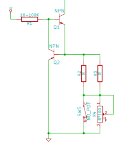
The guts of the circuit is this bit of schematic which is a pretty common and clever way to make a reliable constant-current sink:
Transistor Q1 is drawn as an NPN but it can also be an N-channel FET; its collector (drain) acts as the main current sink for driving all the LEDs. Its base (gate) is driven by R1 which just needs to be a low enough resistance to let the transistor turn on with at least as much current as desired[1. On the order of, say, 50mA / hfe which would typically be at least 100, so around 50mA/100 = 0.5mA; at 5V drop, that would be around 5V/0.5mA = 100KΩ]. Current flows to ground out the emitter (source) through the R2/R3/R4/SW5 resistor network. The target current is defined by the base-emitter voltage (Vbe) of Q2[1. Q2 must be an NPN bipolar transistor for this characteristic.] and the resistor network. Since Vbe is basically constant at around 0.7V, the target current is set by Ohm's law on the resistor network, and when Q2 turns on, current through the collector-emitter junction bypasses the the base (gate) of Q1 which reduces the current flowing until it reaches equilibrium.
I set it up primarily for use with small LEDs that typically expect about 20mA. Ohm's law on the resistor network at 0.7V means I = 0.7V / R. Some options for the value of R2 (omitting R3) or running R2 and R3 in parallel for common resistors are:
- 100Ω @ 0.7V = 7mA @ 4.9mW
- 150Ω || 150Ω = 75Ω @ 0.7V = 9mA @ 3.3mW * 2
- 120Ω || 120Ω = 60Ω @ 0.7V = 12mA @ 4.1mW * 2
- 51Ω @ 0.7V = 14mA @ 10mW
- 39Ω @ 0.7V = 18mA @ 13mW
- 33Ω @ 0.7V = 21mA @ 15mW
- 22Ω @ 0.7V = 32mA @ 22mW
- 15Ω @ 0.7V = 47mA @ 33mW
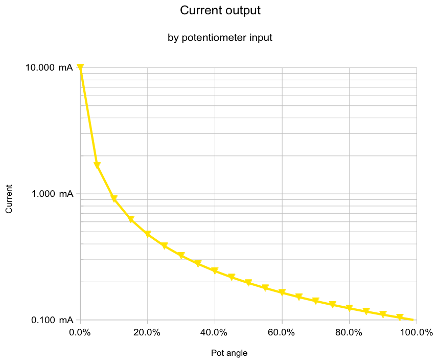
If you're not going to use a potentiometer, bridge the solder jumper labeled NO_POT on the board. Otherwise, you can add in a pot so you have a variable current output. I built up a spreadsheet and found that using a pot with 100x the resistor value offered a good trade off of range and linearity. Here's the output for a 100Ω fixed resistor and a 10K pot:
Ideally this line should be linear on a log scale like this, since an LED's output is proportional to current, and perceived light output has a logarithmic response, so a 50% turn of the pot would appear 50% dimmer, etc. The line gets straighter as the pot's value approaches the fixed resistor, but the range is severely curtailed.
Oh yeah, the pot is pretty crazy looking hole-wise. It's designed to fit a bunch of different salvaged pots, from multi-turn packages to a couple tripod-legged types, to some other weird ones. Basically the row of 3 center holes is for the wiper and all the holes on the left are connected together for the clockwise end, and all the holes on the right are connected together for the counterclockwise end, so whatever hole fits, use that one. There's space for side-entry multi-turn pots, but I think the LEDs get in the way. I was basically wanting any old generic single-turn trim-pot.
Anyway, this same "trick" of using Q2's Vbe can be accomplished with higher accuracy using an op-amp to measure any desired voltage, and this might be a case where a potentiometer to fine-tune the current would be valid. See, a quirk of this circuit, though, is that heat causes Vbe to drop, so as Q2 heats up, the current starts to sag. The limit is about 0.4V, so the current drops proportionally as low as 60% of its original target. A way to use this is to thermally couple Q2 to the output LED or to Q1 so any excess heat will tend to shut down the flow of current and avoid runaway conditions. Of course, with these small currents, heat would only be an issue in a hot enclosure.
Q1 and Q2 are thru-hole transistors only since I have a bunch from salvage and, at these currents and voltages, nearly any NPN at all will work. I arranged the pins in a triangle so you should be able to fit any pin sequence (BCE, CEB, or EBC and then ECB, BEC, or CBE by bending the center pin the other way.) I might throw on the SOT23 surface-mount packages as well in the next go-around.
The other half of the circuit is really just LEDs connected in series. I batched them in binary form—a group of 1, a group of 2, of 4, and of 8—and then inserted bypasses for each group. That way you can select anything from 0 to 15 LEDs in series. I also put in footprints for both 0603 LEDs and thru-hole 5mm. On the layout, the LEDs are labeled with their series count, and bridging the solder jumper labeled NO_1 will short around the "1" LED, NO_2 will short around both the "2" LEDs, etc. I also designed it pretty symmetrical so "1" is in the middle, "2" fills in the corners, "4" alternates between the first 3, and "8" goes around the opposite side[1. With the thru-hole ones, you can always solder them to the other side of the board, but the SMDs are fixed on opposite sides.].
For example, if you wanted to use 5 LEDs, you'd want to insert an LED where it's marked "1" and the other 4 LED's where each spot is marked "4", then bridge "NO_8" and "NO_2" to complete the circuit from IN+ to the collector (drain) of Q1.
For power, there is a spot to solder in a MicroUSB connector (specifically a Molex 105017-0001, but others likely fit), pads for 9V battery connection using Keystone #593 and #594 battery snaps, and two holes that can accommodate up to 18ga wire. I don't know when I'd ever actually use all 15 LEDs, since even at 2 volts each that's 30 volts. With a 9V battery, you'd be lucky to get 4 LEDs in series, and at 5V (e.g. USB), only one white or blue, or 2 red. At least there's some flexibility.
If you wanted to use it as an isolated current source, note that the cathode of the lower-right LED "8" is connected right to the collector (drain) of Q1 so you can just bodge a wire right onto that point.
Finally, all the positive power inputs are copper-poured together and there's a spot for a capacitor if you want it (either 0.1" spacing or 0.2" spacing with 2 holes negative and the one marked "+" positive.) The rest of the circuit is on its own copper pour with a single 8 mil trace connecting it to the power input that is designed to act as a kind of fuse (right near the 10K–100K R1). I removed the soldermask a bit too generously around it on the first iteration but it should work. In theory, you should never be able to blow it, but I'd rather see a little trace like that pop than a power supply or something in case of a bad wiring job.
Note that even if there are no LEDs installed, there is still a current path through R1, Q1, and the resistor network. The small draw will be dominated by R1 (e.g. Vin/R1), and if you use a FET, there is virtually no gate current at all.


Recent Comments